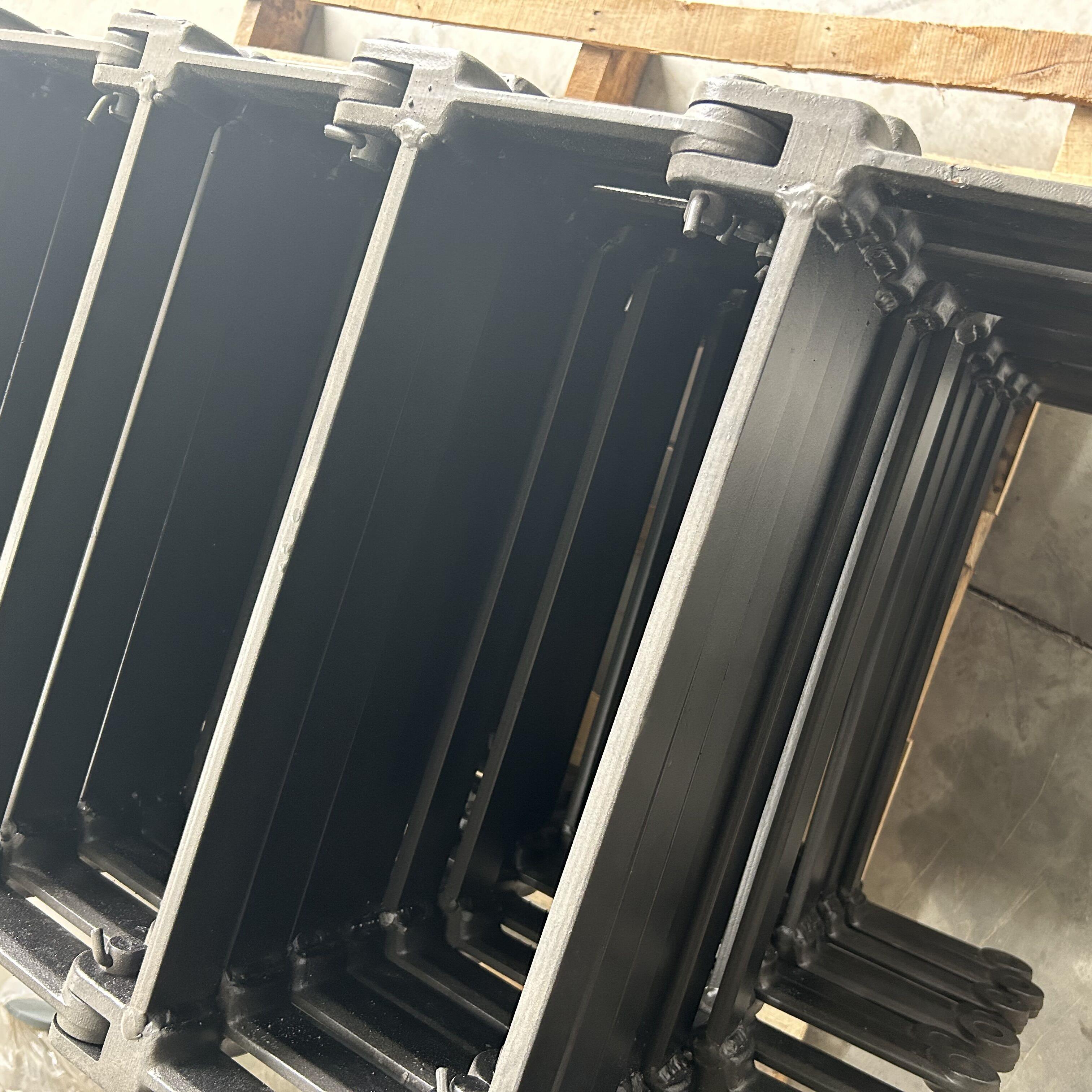
Blog

Spin-EPR-pair separation by conveyor-mode single electron shuttling in Si/SiGe | Nature Communications

Thank you for visiting nature.com. You are using a browser version with limited support for CSS. To obtain the best experience, we recommend you use a more up to date browser (or turn off compatibility mode in Internet Explorer). In the meantime, to ensure continued support, we are displaying the site without styles and JavaScript.

Nature Communications volume  15, Article number: 1325 (2024 ) Cite this article Bulk Material Handling Systems

Spin-EPR-pair separation by conveyor-mode single electron shuttling in Si/SiGe | Nature Communications

Long-ranged coherent qubit coupling is a missing function block for scaling up spin qubit based quantum computing solutions. Spin-coherent conveyor-mode electron-shuttling could enable spin quantum-chips with scalable and sparse qubit-architecture. Its key feature is the operation by only few easily tuneable input terminals and compatibility with industrial gate-fabrication. Single electron shuttling in conveyor-mode in a 420 nm long quantum bus has been demonstrated previously. Here we investigate the spin coherence during conveyor-mode shuttling by separation and rejoining an Einstein-Podolsky-Rosen (EPR) spin-pair. Compared to previous work we boost the shuttle velocity by a factor of 10000. We observe a rising spin-qubit dephasing time with the longer shuttle distances due to motional narrowing and estimate the spin-shuttle infidelity due to dephasing to be 0.7% for a total shuttle distance of nominal 560 nm. Shuttling several loops up to an accumulated distance of 3.36 μm, spin-entanglement of the EPR pair is still detectable, giving good perspective for our approach of a shuttle-based scalable quantum computing architecture in silicon.

Silicon-based electron-spin qubits show single- and two-qubit gate1,2,3,4,5,6,7, as well as readout8,9 fidelities reaching the prerequisite for topological quantum error correction5. This pronounces the need to increase the number of spin-qubits on a chip in an architecture which does preserve the qubit’s manipulation and readout performance. New qubit readout strategies10,11 and ideas for architectures with sparse12 and dense13,14,15 qubit-grids have emerged. Sparse qubit grids have good perspective to eliminate qubit cross-talk issues of their dense counter-part16 and to solve the signal-fanout problem17 by employing tiles of on-chip control-electronics12,18,19. Sparse qubit architectures require high-fidelity coherent spin couplers that can bridge distances of several micrometers. One type of coupler involves high-impedance superconducting resonators, which necessitate a complex interface between spin and the electrical-dipole20,21. Other demonstrations focus on spin-qubit shuttling of one spin-qubit towards another qubit across an array of tunnel-coupled static quantum dots (QDs) named bucket-brigade shuttling22,23,24,25. This approach, however, is complicated by the sensitivity of adiabatic Landau-Zener transitions to potential disorder in the quantum well26.

In this respect, spin shuttling using a moving QD-referred to as conveyor-mode shuttling-is more scalable, as it requires only four easily tunable input signals, independent of its length26,27. While coherent spin shuttling preserving entanglement has been demonstrated with surface acoustic waves in piezoelectric materials28, an array of top-gates connected to four gate sets can induce a moving QD in a Si/SiGe one-dimensional electron channel (1DEC)26. A spin qubit shuttle device (SQS), also called QuBus, employing the conveyor-mode shuttling in Si/SiGe has been demonstrated, with a shuttle distance of 420 nm and a charge shuttling fidelity of (99.42 ± 0.02)%27. Subsequent improvements pushed the cumulative shuttle distance to 19 μm with a charge shuttling fidelity of (99.7 ± 0.3)%29.

Here, we go one step further and characterise the spin-coherence of a SQS operated in conveyor-mode. To probe the spin-coherence, we initialize the SQS by creating a spin-entangled Einstein-Podolsky-Rosen (EPR)-pair at one end. Since the EPR-pair represents a simple example of a fully entangled two particle state30,31, it is ideal to probe the coherence properties of our shuttling procedure. We separate the EPR-pair by conveyor-mode shuttling at a variable distance and velocity and combine them to detect the preservation of the spin-entanglement by Pauli-spin blockade (PSB).

Compared to previous work27, we increased the shuttle velocity by four orders of magnitude to 2.8 ms−1 while preserving the charge shuttle fidelity at (99.72 ± 0.01) % over a distance of nominal 560 nm in total. By observing coherent oscillations from singlet (S) to unpolarised triplet (T0) during the shuttle process, we demonstrate the coherence of the shuttled spin-qubit up to a cumulative distances of nominal 3.36 μm. The dephasing time \({T}_{2}^{*}\) of the EPR-pair is initially on par with ST0 dephasing in a tunnel-coupled double quantum-dot (DQD) in Si/SiGe with a natural abundance of isotopes32. We observe an increase of \({T}_{2}^{*}\) with the shuttle distance, which demonstrates the predicted enhancement of the dephasing time of the shuttled qubit by motional narrowing26. This motional narrowing is caused by averaging out quasistatic noise of the spin’s Zeeman splitting due to its motion, leading to an increased spin-dephasing time26,33.

First, we introduce the SQS device and the experimental methods. The three metallic (Ti/Pt) gate-layers of the SQS device (Fig. 1a) are isolated by conformally deposited 7.7 nm thick Al2O3 and fabricated by electron-beam lithography and metal-lift off on an undoped Si/Si0.7Ge0.3 quantum well with natural abundance of isotopes similar to Ref. 27. The 1DEC of the SQS is formed in the Si/SiGe quantum well by an approximately 1.2 micron long split-gate with 200 nm gate spacing (purple in Fig. 1a). Seventeen so called clavier gates are fabricated on top with 70 nm gate pitch. Eight gates are fabricated on the second gate layer labelled P1, P8, 3 × S1 and 3 × S3. Nine gates are on the third layer labelled B1, B2, B8, B9, 3 × S2 and 2 × S4. Characteristic for our SQS in conveyor mode, the shuttle gates S1, S2, S3, S4 each represent one of the four gate-sets containing two to three clavier gates. Clavier gates of one gate set are electrically connected and thus always on the same electrical potential26,27. Since every fourth clavier gate is on the same potential within the shuttle section, the period λ of the electrostatic potential is 280 nm. The SQS contains two single electron transistors (SETs) at both ends which are used as electron reservoir and proximate charge sensors sensitive to the electron filling at the ends of the SQS. Due to a broken clavier gate B8 on the right side of the device, only the left side of the SQS is used.

a False-coloured scanning electron micrograph of the device used in the experiment showing a top-view on the three metallic layers (1st purple, 2nd blue, 3rd green) of the SQS and their electrical connection scheme. At both ends are single-electron transistors (SETs) formed in the quantum well by gates LB1, LB2, and LP (RB1, RB2, and RP, respectively) on the second gate layer with the current path induced by the yellow gates on 3rd layer. b Typical voltage-pulse sequence for a shuttling experiment, separated into the EPR-pair initialisation, shuttling of one qubit forward and backward and the entanglement detection. c Charge stability diagram recorded by the left SET current ISET with labels for the absolute electron filling of the outermost left DQD of the SQS. The red dotted lines indicate boundaries of the PSB region. Labelled circles indicate voltages on B2 and P1 and correspond to the ones of b. Arrows indicate pulse order.

Figure 1b shows the simplified sequence for a shuttling experiment (details in the method section). It starts with loading four electrons from the left tunnel-coupled SET into the SQS. Then, we decouple this electron reservoir by raising B1, such that the four electrons are trapped in the first QD confined by gates B1 and B2. Next, we form a DQD under P1 and S1 with B2 controlling the inter-dot tunnel coupling. We initialise the electron system to a spin-singlet state by waiting in (n, m) = (4, 0) (stage I) for approximately 1 ms, where n and m are the electron filling numbers of the left and right QD, respectively. Then, we adiabatically pulse to the (3,1) charge state (stages I → S) and close the DQD’s tunnel barrier via B2 (S → T in Fig. 1b, c).The electron in the right QD forms a spin-singlet with the remaining three electrons. We load four electrons into our system to enhance the energy splitting between singlet and triplet states and thus increase the PSB region in gate space (Fig. 1c)16. The analogy to the two-spin EPR-pair is reasonable, since the simple picture holds that two of the three electrons fill one valley-orbit shell and the remaining electron is in a singlet state with the electron in the right QD34.

Afterwards we initiate the electron shuttling process by applying sinusoidal voltage pulses on the shuttle gates S1-S4 (see details in the method section). During shuttling, the three electrons remain confined in the outermost left QD and only the separated electron is shuttled in a moving QD. After shuttling forward and backward by the same distance (Fig. 1b), we increase the tunnel coupling within the DQD again and tune the DQD into PSB (stages T → S → P in Fig. 1b, c). In this way, only the EPR pair in singlet state can tunnel into (4,0) charge state. For all three triplet states this charge transition is energetically forbidden. Finally, we close the barrier once more to freeze the charge state35 (stage F in Fig. 1b, c) and read it out by the current ISET. A detailed explanation of the pulse stages S, T, P and F is given in Supplementary Fig. 4.

In this section, we demonstrate coherent shuttling by measuring ST0 oscillations as a function of shuttle velocity vS, distance d and two values of the global magnetic fields B (Fig. 2a, b). For each measurement of the singlet probability PS, 50000 shuttle cycles are evaluated. Note that the QD shuttles a distance d always twice, forward and backward. We apply a simple sinusoidal signal of frequency f to the gates S1, S2, S3 and S4 (see method section Charge Shuttling for the details), thus the shuttle velocity should be approximately constant and the electron shall be in motion throughout the entire shuttle process, from initialisation to readout. The total shuttle time τS is adjusted by varying the shuttle velocity vS = fλ. The maximum velocity is \({v}_{\max }=2.8\,{{{{{{{{\rm{ms}}}}}}}}}^{-1}\) and the amplitude of the sinusoidal signals is chosen to be in the regime of large charge shuttling fidelity \({{{{{{{{\mathcal{F}}}}}}}}}_{C}=(99.72\pm 0.01)\,\%\) across a shuttle distance d = λ (see methods section Charge Shuttling). We managed to extend this distance to d = 1.2λ = 336 nm finally limited by a drastic drop in electron return probability. The upper bound of vS does not allow to access data points in the grey triangular areas (labelled with τS) of Fig. 2a, b at small τS and large d.

a, b ST0-oscillations as a function of the shuttling time τS and the qubit shuttle distance d at B = 0.8 T (panel a) and B = 0.6 T (panel b), respectively. c: Least-square fit to the data in panel a. d: Least-square fit to the data in b. e Frequencies extracted from the fit in c. The two frequencies are plotted with their corresponding a<,> encoded in the dot size. f: Ratio of the upper and lower frequency for each magnetic field. g Ensemble spin dephasing time \({T}_{2}^{*}\) of the EPR pair as a function of shuttling distance with 1σ-error. Red and purple lines represent least-square fits of two different fit functions. h: Singlet probability PS recorded after shuttling for 0.5D periods of cumulative distance. The time τS + τDQD is the sum of the shuttle time τS and the time of recording the ST0-oscillations in the DQD τDQD. For clarity, traces are offset and amplitude is scaled for purple data points (D = 8λ, D = 10λ and D = 12λ), for which a zoom-in version is plotted in Supplementary Fig. 2.

We fit each line of measured ST0 oscillations for both B (Fig. 2c, d) with

where PS is the probability of detecting the EPR pair in a singlet state, \({T}_{2}^{*}\) is the ensemble dephasing time of the EPR pair, a<,>, ν<,>, φ<,> and c are the visibility, frequency, phase and offset of the ST0-oscillations, respectively. Variations in the offset c may arise from singlet initialisation and detection errors and randomly fluctuates among scan-lines. We empirically find that the data can be best fitted by two oscillations, hence the two cosine terms with their respective frequencies and phases are used. We speculate that this might result from initialising a mixed valley state, as there has been two slightly different spin resonances observed in the presence of a mixed valley-state before34,36. Our fits (Fig. 2c, d) match the measured raw-data in Fig. 2a, b well.

First, we discuss the fitted ν<,>. The origin of the measured ST0-oscillations is the Zeeman energy difference between the spin in the shuttled QD and the spin in the static QD, which is filled by three electrons. The difference originates from slightly different electron g-factors Δg and Overhauser-energies ΔEhf due to hyperfine contact interaction37. This is the same mechanism that leads to ST0 oscillations in the case of a DQD without any conveyor-mode shuttling. These oscillations, which are effectively at d = 0 nm, are discussed in the method section about Singlet-Triplet oscillations. The dynamics of the nuclear spins is slow compared to a shuttle pulse sequence, but the Overhauser field might vary along the 1DEC. The electron g-factor depends on valley state and QD confinement and might vary for the moving QD along the 1DEC as well34. Hence, the Zeeman energy difference of the entangled spins and thus the ST0 oscillation νi frequency depends on the position x of the moving QD. As this position is changing during the shuttle process, the frequency νi(d) becomes a function of shuttle distance d and it is given by an average over the shuttling distance d:

where h is the Planck constant, and μB is the Bohr magneton. We idealize by neglecting the time-dependence of ΔEhf and Δg and by assuming a deterministic thus reproducible trajectory x(t) of the shuttled QD, when averaging over several shuttling cycles. Due to the integral, we expect that changes in νi(d) smooth out for increasing d. Indeed, we observe a shuttle-distance dependence of the ST0 oscillation with a smoothing trend towards larger d (Fig. 2e). Furthermore, we observe that the ν<,> scale with the external magnetic field, which underlines the origin of our observed oscillations being spin-dynamics in agreement with Eq. (2). Calculating pairwise the ratios of ν< and ν> measured at B = 0.6 T and B = 0.8 T, we arrive close to the expected ratio of 0.75 (Fig. 2f). This demonstrates the linearity in magnetic field strength and indicates that the contribution of ΔEhf(x) is small compared to the contribution of the electron g-factor difference. Furthermore, it shows the two oscillation components have distinct, but reproducible Δg(x). For small d, the difference of ν<,> is small increasing the fitting error, but deviations from the ratio 0.75 cannot be fully excluded here. The fitted φ<,> are plotted in the Supplementary Fig. 1.

Most important is the evaluation of the ensemble spin dephasing time \({T}_{2}^{*}\) of the EPR-pair as a function of d, since it contains information on the impact of conveyor-mode shuttling on the spin dephasing. We observe that \({T}_{2}^{*}\) increases with larger shuttle distance (Fig. 2g). Since qubit shuttling opens up new dephasing mechanisms26, this result might be surprising at first sight, but is expected due to a motional narrowing enhancement of the shuttled qubit dephasing time26. We quantify the phenomenon by the fit f1(d) in Fig. 2g using

To incorporate the dependence of Gaussian decay \({T}_{2}^{*}\) of the EPR-pair on shuttle distance d, we use the quadratic addition of inverse \({T}_{2}^{*}\) times for the left (L) and right (R) electron spin and include a factor for motional narrowing for the shuttled qubit, where \({T}_{2,\,{{\mbox{L}}}\,}^{*}\) is the ensemble spin dephasing time of the electron-spin that remains static in the outermost left QD, and \({T}_{2,\,{{\mbox{S}}}}^{*}(d)\equiv {T}_{2,{{\mbox{R}}}\,}^{*}\sqrt{\frac{d+{l}_{c}}{{l}_{c}}}\) represents the ensemble spin dephasing time of the forward and backward shuttled electron spin (total distance 2d), averaging over a d long spatial range of quasistatic-noise of its Zeeman-energy Ez(x(t)) having a correlation length lc26. Note that the motional narrowing is independent of vS for noise being quasi-static on the time-scale of the shuttle, but it depends on the shuttled distance and thus the ensemble volume participating in averaging out the quasi-static noise. We distinguish between the static ensemble dephasing times \({T}_{2,\,{{\mbox{L}}}\,}^{*}\) and \({T}_{2,\,{{\mbox{R}}}\,}^{*}\) , since we expect the confinement strength within the static QD to be less than in the moving QD. Our fit to the ensemble dephasing time of the EPR pair (Fig. 2g) results in \({T}_{2,\,{{\mbox{L}}}\,}^{*}=(1110\pm 90)\) ns, \({T}_{2,\,{{\mbox{R}}}\,}^{*}=(520\pm 20)\) ns and lc = (13 ± 3) nm. This in total yields \({T}_{2,\,{{\mbox{S}}}\,}^{*}(280\,{{{{{{{\rm{nm}}}}}}}})=(2460\pm 310)\,{{{{{{{\rm{ns}}}}}}}}\) . This result implies that shuttled qubit increases its dephasing time by a factor of ≈ 4 when shuttled twice across a distance of nominal 280 nm due to motional narrowing. Note that the data points in Fig. 2g tend to be lower than the fit for the largest d, which might be due to dephasing mechanisms induced by the shuttle process such as motion-induced valley excitations26. At very short shuttle distance d, a deformation of the moving QD might add to the change in spin dephasing time. Assuming a constant shuttle velocity, constant shape of the moving QD and only motional narrowing of Ehf(x), we derive the fit function f2(d) exhibiting a modified motional narrowing factor (Fig. 2g). Remarkably, we arrive at very similar fitting parameters (see Supplementary note 1).

In order to increase the distance of shuttling, we always shuttle at a maximum velocity \({v}_{\max }\) and once the shuttled electron returns to the right QD of the DQD (stage S), we recorded the ST0 oscillations by waiting between additional 0 to 1 μs prior to measure the EPR spin-state. We plot the spin-singlet probability PS of the EPR-pair as a function of the total time τS + τDQD of shuttling (τS) and waiting (τDQD) (Fig. 2h). Due to the limited length of the shuttle zone, we increase the cumulative distance by shuttling in- and out for one period λ multiple times. The total number of periods (D) shuttled forward plus backward is indicated on the left as the accumulated shuttle distance. For example for the trace labelled D = 2, the voltage pulses applied to S1-S4 are designed to shuttle the electron one period λ = 280 nm forward and same distance back towards the spin-detector. For D = 1, the electron is shuttled half a period forward, and the same distance back towards the detector. Strikingly, we still observe ST0 oscillations for the trace labelled D = 12, for which the electron shuttles alternating six times forward and backward by λ being nominally equivalent to an accumulated distance of 3.36 μm. The appearance of ST0 oscillations show that the EPR-pair remained entangled after such long shuttling distance.

Coherent shuttling of a spin qubit and EPR separation allows us to collect information about Δg(x) along the SQS. Instead of shuttling the spin-qubit forward and backward with a τS-dependent vS, we shuttle it by a distance x along the 1DEC at maximum \({v}_{\max }=2.8\,{{{{{{{{\rm{ms}}}}}}}}}^{-1}\) , wait there for a time τW to let the ST0 oscillations evolve and then shuttle back at maximum vS for PSB detection. We observe (Fig. 3) ST0-oscillations and similar to Fig. 2a, b, their frequency ν(x, B) scales with the B-field as expected (cmp. Figure 3a and b). Compared to Fig. 2a, b, ν(x, B) tend to fluctuate faster as a function of x. This is expected, since ν<,> results from averaging many positions x(t) in the coherent shuttle experiment (Eq. (2)) in Fig. 2, while here ν dominantly depends on the fixed position x. Note that x(t) and thus d is not measured in any case, but deduced from the expected position of the ideal propagating wave potential \(x=\lambda \frac{{{\Delta }}\varphi }{2\pi }\) , where φ is the phase of the voltages applied to gates S1-S4 relative to the initialisation potential. Hence, we neglect potential disorder and wobbling effects of the propagating wave potential, which are exemplary simulated in Ref. 26. Notably, ν(x) starts to become nearly constant at x > 210 nm. This could be an indication that the electron stops moving at this point. If we try to shuttle to x > 330 nm > λ, the electron dominantly does not return, indicating potential disorder which is sufficiently high to break the QD confinement in the propagating QD.

a False-colour plot of the measured Singlet return probability measured at B = 0.8 T. b Same as in a with B = 0.5 T.

This work shows progress on electron shuttling in conveyor-mode, building up on earlier demonstrations of charge shuttling27. We improved the shuttle velocity by four orders of magnitude to a regime at which coherent shuttling becomes feasible26. When moving into and out of the device once, we demonstrate coherent shuttling by EPR pair separation and recombination across a total distance of nominal 560 nm and at least 420 nm in case the electron spins halts at x = 210 nm. Furthermore, we detect entanglement when moving the electron for an accumulated shuttle distance of nominal 3.36 μm (at least 2.4 μm). Remarkably, the dephasing time of the shuttled qubit \({T}_{2,\,{{\mbox{S}}}\,}^{*}\) is enhanced by motional narrowing, while the static electron-spin dominates the dephasing of the spin-entangled EPR-pair. Based on the fitted \({T}_{2,\,{{\mbox{S}}}\,}^{*}(280\,{{{{{{{\rm{nm}}}}}}}})\approx 2460\,{{{{{{{\rm{ns}}}}}}}}\) ( ≈ 2130 ns for fitting with f2(d)), we can estimate a phase-infidelity caused by the shuttle time τS at maximum shuttle velocity vS using the Gaussian decay

We estimate a shuttling-induced phase-infidelity of \(1-{{{{{{{\mathcal{F}}}}}}}}=(0.66\pm 0.17)\) % for a total shuttle distance of nominal 2d = 2λ = 560 nm (at least 420 nm). Assuming a constant shuttle velocity, constant shape of the moving QD and only motional narrowing of Ehf(x) (fit equation f2(d) see supplementary material) yields a matching infidelity of \(1-{{{{{{{\mathcal{F}}}}}}}}=(0.88\pm 0.18)\) % within the error range.

Next, we have to increase the shuttle distance by improving confinement of the moving QD. The competing electrostatic potential disorder can be reduced by replacing Al2O3 by SiO2, which exhibits less interface defects, and by thinner dielectric layers26. We already achieved a charge shuttle fidelity of (99.7 ± 0.3)% for total shuttle distance of 19 μm in a 10 μm long Si/SiGe QuBus29. The spin dephasing time can be enhanced by isotopically purified 28Si and valley excitations can be mitigated by higher valley splitting38. Conversely, the valley splitting can be mapped in the shuttle region39. Adding spin-manipulation zones will grant more flexibility in performing coherent shuttling experiments to explore the dephasing channels and the role of the valley states. In the long run, we target at the integration of our spin shuttle device into a scalable semiconductor qubit architecture40.

A prerequisite for spin-coherent shuttling is that the electron stays confined in the moving QD, which we call charge shuttling. Figure 4 depicts the pulse procedure for benchmarking the charge shuttling in the same device that we used for spin-coherent shuttling. Firstly, we load four electrons into the first QD by lowering B1 (Fig. 4a inset). Due to cross-talk, we need to compensate on P1 and B2. Thereafter, the barrier is raised again to isolate the system. Loading takes approximately 2 ms time as the voltage on B1 is 10 kHz lowpass-filtered. Subsequently, one electron is moved into the second QD (Fig. 4a, red triangle → S) and the barrier B2 is closed by pulsing it down by 120 mV (S → T). After stage T, the shuttle pulse (Fig. 4b lower part) is applied to the gate-sets S1 − S4

The amplitudes (U1, U3) applied to the gate-sets S1 and S3 on the second layer (blue in Fig. 1a) is Ulower = 150 mV, whereas the amplitudes (U1, U3) applied to the gate-sets S2 and S4 on the 3rd metal layer is slightly higher (Uupper = 1.28 ⋅  Ulower = 192 mV) to compensate for the difference of capacitive coupling of these layers to the quantum well. This compensation extends to the DC-part of the shuttle gate voltages. The maximum amplitude is limited to 192 mV due to the attenuation installed in the cryostat together with the maximum peak-to-peak output amplitude of the arbitrary waveform generator of 5 V. The offsets C1 = C3 = 0.7 V are chosen to form a smooth DQD, whilst C2 = C4 = 0.896 V are chosen to form a smooth DC potential. The phases are chosen to build a travelling wave potential across the one-dimensional electron channel (φ1 = − π/2, φ2 = 0, φ3 = π/2, φ4 = π). This travelling wave potential is illustrated in Fig. 4b at the top part. The barrier B2 is pinched off to limit the cross-talk-influence from the shuttle pulse to the static electrons. The electron is moved adiabatically by one period of the travelling wave potential (280 nm) to the right. After one period, the absolute gate voltages are exactly identical to the prior state, when the charge scan in Fig. 4a has been recorded. Hence, we can check whether the electron is shuttled away by going back to the electrostatic configuration corresponding to the red triangle and measuring the SET current. By time reversing the voltage pulses on S1 − S4, we shuttle the electron back and perform a measurement in a similar manner (detailed description of time reversed pulses in Supplementary Fig. 3). Then, we calculate a histogram as shown in the inset of Fig. 4e, fit two Gaussian distributions and take the fits crossing point to define the range of ISET assigned to three and four electron detection events. Only if the first measurement yields three (i.e. electron is shuttled away from detector) and the second measurement four electrons (i.e. electron is shuttled back to detector), a shuttling event is counted as successful. The same approach for counting successful charge shuttle events has been used in Ref. 27.

a Charge scan of the DQD under gates P1 and S1 with labelled electron filling. Voltage pulse (red triangle → S → T) of the initialisation in (3,1) is marked (Stage T is at B2 = 0.7 V). Inset: Schematic of the electrostatic potential along the 1DEC under gates B1, P1 and B2 for loading. The respective electrostatic configurations are marked with red and blue triangles. b Shuttle Pulse. Schematic of the electrostatic potential under the labelled gates after initialisation (top). Sinusoidal voltage pulse VSi(τS) applied to S1 − S4 to shuttle the electron one period (λ = 280 nm) forward (bottom). c Flowchart of the charge shuttling experiment. Labelled points correspond to panels a and b and Fig. 1b. Coloured arrows in the load and shuttle sections express that during this part of the pulse other gates than P1 and B2 are pulsed. The pulse stages M and red triangle are electrostatically the same. d Charge shuttling fidelity as a function of shuttle pulse amplitude Ulower at f = 10 MHz. e Charge shuttle fidelity as a function of the shuttle pulse frequency f at Ulower = 150 mV. Inset: Histogram of SET-currents measured during point M with assigned filling numbers of the QD underneath gate P1.

In Fig. 4d, we plot the charge shuttling fidelity \({{{{{{{{\mathcal{F}}}}}}}}}_{C}\) as a function of the lower layer amplitude Ulower, the upper layer amplitude is Uupper = 1.28 ⋅  Ulower to compensate for the larger distance to the 1DEC. We find a steep rise of \({{{{{{{{\mathcal{F}}}}}}}}}_{C}\) at Ulower > 110 mV. The histogram of ISET for all Ulower > 125 mV (inset of Fig. 4e) shows well separated Gaussians assigned to either four or three electron filling of the QD underneath gate P1. Due to nonlinear effects on the SET, the peak for four electrons is narrower than the peak for three electrons. Figure 4e shows charge shuttling fidelities as a function of shuttle frequency f as defined in Eq. (5) which corresponds to a shuttle velocity vS = fλ. From the green points we read off high fidelities up to 10 MHz (2.8m/s), presumably limited by electrostatic disorder in the 1DEC. By averaging \({{{{{{{{\mathcal{F}}}}}}}}}_{C}({U}_{{{{{{{{\rm{lower}}}}}}}}} > 125\,{{{{{{{\rm{mV}}}}}}}})\) in Fig. 4d, we calculate the mean charge shuttling fidelity for shuttling a nominal total distance of 2λ = 560 nm (λ forwards and backwards) to be \({{{{{{{{\mathcal{F}}}}}}}}}_{C}=(99.72\pm 0.01)\,\%\) . This value is slightly better than the charge shuttling fidelity of 99.42% obtained in Ref. 27. Moreover, we found charge shuttling across 2λ and back at f = 2 MHz. We tracked the charge by measuring the charge state after every shuttle-pulse, which moves the electron by one period λ (cmp. shuttle tomography method in Ref. 29) and calculated a transfer fidelity of 98.7% at the same voltage amplitudes.

To demonstrate that the single-electron spin-qubit coherently shuttles, we use the preservation of the entanglement with the static electron spin, which we detect by the coherent oscillations between spin-singlet S and unpolarised spin-triplet T0 state of this EPR pair

in the \((\left\vert {{{{{{{\rm{S}}}}}}}}\right\rangle,\left\vert {{{{{{{{\rm{T}}}}}}}}}_{0}\right\rangle )\) -basis. Here, J(ε) represents the exchange interaction as a function of the detuning ε( = VP1) between the left and right QD. Δg is the g-factor difference between the two QDs26,34. ΔEhf is the Overhauser-energy-difference between the two dots. After loading four electrons as shown in Fig. 4a, we initialise the system to S(4,0) by waiting at stage I (Fig. 5a) for 2 ms. Next, we step VP1 by 20 mV which reduces J(ε) and turns on ΔgμBB by letting one electron adiabatically tunnel into the right QD. As the two electrons are laterally separated, they are subject to different electron g-factors resulting in different Zeeman-energies as a result of the global B-field of 0.8 T. At stage S, we wait for τDQD time and pulse to the PSB in stage P where spin information is converted to charge information. The conversion takes approximately 500 ns after which a raise of the inter-dot barrier freezes the charge state for readout (stage F). Iterating over this pulse scheme, we record the singlet return probability PS (Fig. 5b), which is fitted by

a Charge stability-diagram of the DQD in Fig. 4a. b ST0-oscillation as a function waiting for time τDQD at stage S. The singlet probability PS is measured by applying the pulse from panel c spending various time τDQD at stage S. The solid line is fit to the data. inset: Readout histogram with threshold (dashed line) determined by the fitted crossing point of the two Gaussians. c Schematic representation of the experiment pulse. Numbers correspond to stages in a and Fig. 4a. d Schematic of the additional stages complementing the pulse scheme in c for doing the spin-shuttling measurement. They slot in panel c in between the separation and the PSB-freeze-RO pulse segments. The SRL section represents any applied shuttle pulse.

We yield for the spin dephasing time of the entangled spin-state \({T}_{2}^{*}=(565\pm 10)\,{{{{{{{\rm{ns}}}}}}}}\) and the frequency ν = (7.29 ± 0.01) MHz. Figure 5c summarises the pulse in a schematic way. For coherent shuttling experiments, instead of waiting at the separation stage the sequence presented in Fig. 5d is inserted between the separation and PSB-freeze-RO pulse segments shown in Fig. 5c.

All experiments are conducted in a dilution refrigerator with a base temperature of 40 mK. All DC lines to the device are filtered by pi-filters (fc = 5 MHz) at room temperature and by 2nd order RC filters with fc = 10 kHz at base temperature. The clavier gates, B2, P1, P8, and B8 are connected to resistive bias-tees with a cutoff frequency of 5 Hz. Signals are applied to the AC and DC input terminal of the bias-tee, in order to allow inclusion of millisecond long pulse segments. A serial resistor is added to the low-frequency terminal, the value of which is tuned by flattening the sensor signal response. The SETs are DC-biased by 100 μV and readout by a transimpedance amplifier and an analog to digital converter.

The data generated in this study have been deposited in the Zenodo database (https://doi.org/10.5281/zenodo.8413694).

Yoneda, J. et al. A quantum-dot spin qubit with coherence limited by charge noise and fidelity higher than 99.9%. Nat. Nanotechnol. 13, 102–106 (2018).

Article  CAS  PubMed  ADS  Google Scholar 

Zajac, D. M. et al. Resonantly driven cnot gate for electron spins. Science 359, 439–442 (2018).

Article  MathSciNet  CAS  PubMed  ADS  Google Scholar 

Watson, T. F. et al. A programmable two-qubit quantum processor in silicon. Nature 555, 633–637 (2018).

Article  CAS  PubMed  ADS  Google Scholar 

Xue, X. et al. Benchmarking gate fidelities in a Si/SiGe two-qubit device. Phys. Rev. X 9, 021011 (2019).

Xue, X. et al. Quantum logic with spin qubits crossing the surface code threshold. Nature 601, 343–347 (2022).

Article  CAS  PubMed  PubMed Central  ADS  Google Scholar 

Noiri, A. et al. Fast universal quantum gate above the fault-tolerance threshold in silicon. Nature 601, 338–342 (2022).

Article  CAS  PubMed  ADS  Google Scholar 

Mills, A. R. et al. Two-qubit silicon quantum processor with operation fidelity exceeding 99%. Sci. Adv. 8, eabn5130 (2022).

Article  CAS  PubMed  PubMed Central  Google Scholar 

Connors, E. J., Nelson, J. & Nichol, J. M. Rapid high-fidelity spin-state readout in Si/SiGe quantum dots via rf reflectometry. Phys. Rev. Appl. 13, 024019 (2020).

Article  CAS  ADS  Google Scholar 

Noiri, A. et al. Radio-frequency-detected fast charge sensing in undoped silicon quantum dots. Nano Lett. 20, 947–952 (2020).

Article  CAS  PubMed  ADS  Google Scholar 

Struck, T. et al. Robust and fast post-processing of single-shot spin qubit detection events with a neural network. Sci. Rep. 11, 16203 (2021).

Article  CAS  PubMed  PubMed Central  ADS  Google Scholar 

Kammerloher, E. et al. Sensing dot with high output swing for scalable baseband readout of spin qubits. Preprint at https://arxiv.org/abs/2107.13598 (2021).

Boter, J. M. et al. Spiderweb array: A sparse spin-qubit array. Phys. Rev. Appl. 18, 024053 (2022).

Article  CAS  ADS  Google Scholar 

Hollenberg, L. C. L., Greentree, A. D., Fowler, A. G. & Wellard, C. J. Two-dimensional architectures for donor-based quantum computing. Phys. Rev. B 74, 045311 (2006).

Lawrie, W. I. L. et al. Quantum dot arrays in silicon and germanium. Appl. Phys. Lett.116 080501 (2020).

Mortemousque, P.-A. et al. Coherent control of individual electron spins in a two-dimensional quantum dot array. Nat. Nanotechnol. 16, 296–301 (2021).

Article  CAS  PubMed  ADS  Google Scholar 

Philips, S. G. J. et al. Universal control of a six-qubit quantum processor in silicon. Nature 609, 919–924 (2022).

Article  CAS  PubMed  PubMed Central  ADS  Google Scholar 

Vandersypen, L. M. K. et al. Interfacing spin qubits in quantum dots and donors-hot, dense, and coherent. npj Quantum Inf. 3, 34 (2017).

Hollmann, A. et al. 30 GHz-voltage controlled oscillator operating at 4 K. Rev. Sci. Instrum. 89, 114701 (2018).

Article  PubMed  ADS  Google Scholar 

Otten, R. et al. Qubit bias using a CMOS DAC at mK temperatures. In 2022 29th IEEE International Conference on Electronics, Circuits and Systems (ICECS), 1–4 (2022).

Landig, A. J. et al. Virtual-photon-mediated spin-qubit-transmon coupling. Nat. Commun. 10, 5037 (2019).

Article  CAS  PubMed  PubMed Central  ADS  Google Scholar 

Borjans, F., Croot, X., Mi, X., Gullans, M. & Petta, J. Resonant microwave-mediated interactions between distant electron spins. Nature 577, 195–198 (2020).

Article  CAS  PubMed  ADS  Google Scholar 

Mills, A. R. et al. Shuttling a single charge across a one-dimensional array of silicon quantum dots. Nat Commun. 10, 1063 (2019).

Article  CAS  PubMed  PubMed Central  ADS  Google Scholar 

Zwerver, A. M. J. et al. Qubits made by advanced semiconductor manufacturing. Nat. Electron. 5, 184–190 (2022).

Yoneda, J. et al. Coherent spin qubit transport in silicon. Nat. Commun. 12, 4114 (2021).

Article  CAS  PubMed  PubMed Central  ADS  Google Scholar 

Mortemousque, P.-A. et al. Enhanced spin coherence while displacing electron in a two-dimensional array of quantum dots. PRX Quantum 2, 030331 (2021).

Langrock, V. et al. Blueprint of a scalable spin qubit shuttle device for coherent mid-range qubit transfer in disordered Si/SiGe/SiO2. PRX Quantum 4, 020305 (2023).

Seidler, I. et al. Conveyor-mode single-electron shuttling in Si/SiGe for a scalable quantum computing architecture. npj Quantum Inf. 8, 100 (2022).

Bertrand, B. et al. Fast spin information transfer between distant quantum dots using individual electrons. Nat. Nanotechnol. 11, 672–676 (2016).

Article  CAS  PubMed  ADS  Google Scholar 

Xue, R. et al. Si/SiGe qubus for single electron information-processing devices with memory and micron-scale connectivity function. Preprint at https://arxiv.org/abs/2306.16375 (2023).

Hensen, B. et al. Loophole-free Bell inequality violation using electron spins separated by 1.3 kilometres. Nature 526, 682–686 (2015).

Article  CAS  PubMed  ADS  Google Scholar 

Stuart, J. et al. Experimental test of local hidden-variable theories. Phys. Rev. Lett. 28, 938 (1972).

Connors, E. J., Nelson, J., Edge, L. F. & Nichol, J. M. Charge-noise spectroscopy of Si/SiGe quantum dots via dynamically-decoupled exchange oscillations. Nat. Commun. 13, 940 (2022).

Article  CAS  PubMed  PubMed Central  ADS  Google Scholar 

Brand, M. A. et al. Precession and motional slowing of spin evolution in a high mobility two-dimensional electron gas. Phys. Rev. Lett. 89, 236601 (2002).

Article  CAS  PubMed  ADS  Google Scholar 

Cai, X., Connors, E. J., Edge, L. F. & Nichol, J. M. Coherent spin-valley oscillations in silicon. Nat. Phys. 19, 386–393 (2023).

Nurizzo, M. et al. Complete readout of two-electron spin states in a double quantum dot. PRX Quantum 4, 010329 (2023).

Kawakami, E. et al. Electrical control of a long-lived spin qubit in a Si/SiGe quantum dot. Nat. Nanotechnol. 9, 666–670 (2014).

Article  CAS  PubMed  ADS  Google Scholar 

Chekhovich, E. A. et al. Nuclear spin effects in semiconductor quantum dots. Nat. Mater. 12, 494 (2013).

Article  CAS  PubMed  ADS  Google Scholar 

Losert, M. P. et al. Practical strategies for enhancing the valley splitting in Si/SiGe quantum wells. Phys. Rev. B 108, 125405 (2023).

Article  CAS  ADS  Google Scholar 

Volmer, M. et al. Mapping of valley-splitting by conveyor-mode spin-coherent electron shuttling. Preprint at https://arxiv.org/abs/2312.17694 (2023).

Künne, M. et al. The spinbus architecture: scaling spin qubits with electron shuttling. Preprint at https://arxiv.org/abs/2306.16348 (2023).

Albrecht, W., Moers, J. & Hermanns, B. HNF - helmholtz nano facility. J. Large-scale Res. Facilities 3, A112 (2017).

We acknowledge the support of the Dresden High Magnetic Field Laboratory (HLD) at the Helmholtz-Zentrum Dresden - Rossendorf (HZDR), member of the European Magnetic Field Laboratory (EMFL). This work has been funded by the German Research Foundation (DFG) under Germany’s Excellence Strategy - Cluster of Excellence Matter and Light for Quantum Computing" (ML4Q) EXC 2004/1 - 390534769, by the Federal Ministry of Education and Research under Contract No. FKZ: 13N14778, and by the National Science Centre (NCN), Poland under QuantERA programme, Grant No. 2017/25/Z/ST3/03044. Project Si-QuBus received funding from the QuantERA ERA-NET CoFund in Quantum Technologies implemented within the European Union’s Horizon 2020 Programme. The device fabrication has been done at HNF - Helmholtz Nano Facility, Research Center Juelich GmbH41.

Open Access funding enabled and organized by Projekt DEAL.

JARA-FIT Institute for Quantum Information, Forschungszentrum Jülich GmbH and RWTH Aachen University, Aachen, Germany

Tom Struck, Mats Volmer, Lino Visser, Tobias Offermann, Ran Xue, Hendrik Bluhm & Lars R. Schreiber

ARQUE Systems GmbH, Aachen, Germany

Tom Struck, Hendrik Bluhm & Lars R. Schreiber

Helmholtz Nano Facility (HNF), Research Center Jülich, Jülich, Germany

Jhih-Sian Tu & Stefan Trellenkamp

Institute of Physics, Polish Academy of Sciences, Warsaw, Poland

You can also search for this author in PubMed  Google Scholar

You can also search for this author in PubMed  Google Scholar

You can also search for this author in PubMed  Google Scholar

You can also search for this author in PubMed  Google Scholar

You can also search for this author in PubMed  Google Scholar

You can also search for this author in PubMed  Google Scholar

You can also search for this author in PubMed  Google Scholar

You can also search for this author in PubMed  Google Scholar

You can also search for this author in PubMed  Google Scholar

You can also search for this author in PubMed  Google Scholar

T.S., M.V. and L.V. conducted the experiments. T.S., M.V., T.O., L.V. and L.R.S. analysed the data. J.T. and R.X. fabricated the device. S.T. wrote the e-beam layers. Ł.C. derived motional narrowing effect of nuclear spins. L.R.S. designed and supervised the experiment. L.R.S and H.B. guided all authors. T.S., M.V., L.V., T.O. and L.R.S. wrote the manuscript, which was commented by all other authors.

Correspondence to Lars R. Schreiber.

Conveyor-mode shuttling is covered by a patent family (EP 4031486, US 2022/0293846 A1, CN114424346 A) by inventors L.R.S, H.B., Künne, Seidler. The patent application, co-owned by RWTH Aachen University and the Forschungszentrum Jülich, is currently pending. Qubit initialization and readout in the shuttle device is covered by patents families (US11687473B2, EP4031489, CN114402441) and (US 2022/0327072, EP4031487, CN114424344) by inventors L.R.S., H.B., Künne, co-owned by RWTH Aachen University and the Forschungszentrum Jülich. US11687473B2 is granted, all other pending. L.R.S. and H.B. are founders and shareholders of ARQUE Systems GmbH. The other authors declare no competing interest.

Nature Communications thanks Kok Wai Chan, who co-reviewed with MengKe Feng and the other, anonymous, reviewer(s) for their contribution to the peer review of this work. A peer review file is available.

Publisher’s note Springer Nature remains neutral with regard to jurisdictional claims in published maps and institutional affiliations.

Open Access This article is licensed under a Creative Commons Attribution 4.0 International License, which permits use, sharing, adaptation, distribution and reproduction in any medium or format, as long as you give appropriate credit to the original author(s) and the source, provide a link to the Creative Commons license, and indicate if changes were made. The images or other third party material in this article are included in the article’s Creative Commons license, unless indicated otherwise in a credit line to the material. If material is not included in the article’s Creative Commons license and your intended use is not permitted by statutory regulation or exceeds the permitted use, you will need to obtain permission directly from the copyright holder. To view a copy of this license, visit http://creativecommons.org/licenses/by/4.0/.

Struck, T., Volmer, M., Visser, L. et al. Spin-EPR-pair separation by conveyor-mode single electron shuttling in Si/SiGe. Nat Commun 15, 1325 (2024). https://doi.org/10.1038/s41467-024-45583-7

DOI: https://doi.org/10.1038/s41467-024-45583-7

Anyone you share the following link with will be able to read this content:

Sorry, a shareable link is not currently available for this article.

Provided by the Springer Nature SharedIt content-sharing initiative

By submitting a comment you agree to abide by our Terms and Community Guidelines. If you find something abusive or that does not comply with our terms or guidelines please flag it as inappropriate.

Nature Communications (Nat Commun) ISSN 2041-1723 (online)

Spin-EPR-pair separation by conveyor-mode single electron shuttling in Si/SiGe | Nature Communications

Inclined Conveyor Design Sign up for the Nature Briefing newsletter — what matters in science, free to your inbox daily.